Old News (Feb 08 - Mar 08)
Finishing off the layout
The layout is complete at this stage. I've spent a bit of time verifying it, but I'm going to do a quick second verification. Once the gerber files are off, it's the stage at which it costs Real Money, and I don't want to get back ten pretty green coasters. They won't even make great coasters, the Spectranet PCB is too small for one of those PCB notepads, or a mug of tea...so it must be absolutely right before it goes to PCB Train. Or at least, right enough that I'm confident PCB problems won't stop it from working.
I've ticked off all the nets by manually selecting each one in PCB (which highlights the selected net in green) then checking against the actual chip data sheets. For all of the chips, I've put in my own pin lists into gSchem, so I could always have made an error as I transferred them from data sheet to schematic.
I want to check the ground and power connections one more time, as well as go through the through connector traces (since the through connector didn't feature in the schematic, and therefore, didn't feature in the netlist created by gschem). Once all the verification is complete, the gerbers will go off to PCB Train, who will undoubtedly tell me I've violated some design constraint (I did put their design rules into PCB, but I've had problems with PCB fabs before where they couldn't cope with some gerber commands that PCB emitted. And I wish the PCB layout software I use wasn't just called 'PCB', it makes the last paragraph incredibly confusing!) Hopefully, anything that PCB Train comes back with won't be a show stopper, and after about 3 weeks, I'll have ten prototype PCBs. The first one, I'll assemble by hand soldering a bit at a time - first the CPLD. Then the flash and RAM. Once that's tested, then the W5100. If it all works, then the remaining PCBs will be used to test ways of economically assembling the boards. Assembly will be some form of reflow (using solder paste) - either with a hot air gun or an oven. If demand looks like being high enough, I'll get solder paste stencils made. Things like the DivIDE, and the more expensive DivIDE+ have all sold at least a hundred copies each, and even if it takes a couple of years to shift that amount, a stencil may make it significantly easier to assemble. If you don't know - a solder paste stencil is basically some thin strong material (mylar or brass) with holes cut or etched into it over each surface mount component's pad. Then all you do is squeegee solder paste over it, and it fills the holes. Remove the stencil, place the components, apply hot air and you're done.
While I'm waiting for the boards, I'll do more on the software prototyping - finish off the gethostbyname() implementation, and then the C library. The C library, being not much more than a wrapper over the assembly language functions, shouldn't take an awful lot of time to do. Then I'll attack the BASIC interpreter again. Garry Lancaster has provided some useful pointers from his experience with ResiDOS, along with the ResiDOS code itself so I can learn from what he did for the parser.
Winston 21:49, 31 March 2008 (BST)
Even more layout
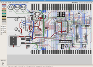
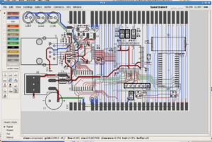
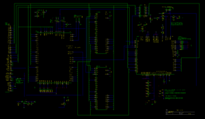
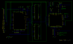
The PCB layout is now complete, bar the shouting. Specifically, all nets are routed (I think! It's late and I'm not gonna start checking them now). Last week, I mentioned the vexed question of the layout issues in the vicinity of the W5100 - these were largely solved by squashing the crystal circuit down a bit and moving surrounding components out a bit to fit the crystal. This allowed just enough space above the crystal to squeeze a track or two. I also had to put a couple of address lines under the W5100, but they are on the solder side and there's a ground plane between them and the chip, and I made sure they crossed the RSET_BG track at right angles (this goes to the PHY's off-chip resistor network).
There was much fiddling needed to route the address and data bus from the CPLD, to the flash memory, to the RAM. I had to use all four layers for routing, it gets extremely dense around the flash and RAM chips - but that's the only place where I had to use the ground plane layer for routing, but it's only a little bit of the ground plane and it won't hurt anything (consider this memory functions fine without a ground plane at all - it's really the CPLD and the W5100 where the ground plane is most important. My W5100 breakout board, which is only two layers, suffers some ground bounce problems).
If you look carefully, you may notice that apart from the through port traces being squeezed down in places to allow some via farms for the address and data bus around the RAM and flash, the input side capacitor to the 3.3v regulator has changed, too. I discovered the +3 does not have 9v exposed at the edge connector, so I am forced to use the 5v line for the 3.3v regulator's supply. I know it works fine (the breadboard prototype does just that), but I had hoped to avoid loading the Spectrum's 7805 (5 volt regulator) down any more than it is. That being the case, I can use a lower voltage surface mount capacitor for the input side, rather than a through-hole electrolytic.
On "twizzling" (which is what people call randomly routing the data and address bus to memory). I am absolutely insistent that the data and address bus lines for the flash chip are exactly as the datasheet says, even if it makes it harder to route. (The DivIDE, by contrast, just routes the address and data bus lines to the easiest pin on the EEPROM). I don't want to have to translate binary files before flashing them, and I don't want to have to figure out what the flash control codes have changed to. When you program flash, you must first write some control bytes to the flash chip to put it in programming mode. So the flash is wired straight. So wiring it for ease of layout is just to invite confusion (especially if there's a problem with the prototype board - I then have to figure out not only if there's an electrical fault - but also if it's a software fault. So I'd rather eliminate the possibility of software faults right now by wiring it straight). But it doesn't matter with the RAM, so although the data bus is wired straight, the address lines are wired in an order that made routing easier.
So now all I need to do is make the silk screen layer more meaningful (label the JTAG connector, label the LEDs), and then go through each net and check it really does connect to the right thing. Although it was laid out with the netlist loaded into PCB, there's always the possibility I mislabeled a pin in the schematic, so I'll painstakingly go through every connection and reference it to the manufacturer's datasheet for each chip.
Winston 23:39, 23 March 2008 (UTC)
Layout
I've started laying out the 'production prototype' PCB. As I predicted, it is a challenge - mainly around the W5100 itself.
If you've never laid out a PCB, you probably don't know this, so I'll expand a bit. Some components are a bit fussy about PCB layout, and the W5100 itself has a few things to be borne in mind while laying out a PCB. To whit:
- Digital traces (address, data bus etc.) should not go near the incoming ethernet TX/RX lines as they come from the magnetics to the W5100.
- There's a general 'exclusion zone' around the magjack itself (the combined RJ45 jack and magnetics).
- Digital lines also should avoid the analogue supply circuit. After all, we've gone to all that effort of putting a 1uH choke and extra decoupling there, it'd ruin all that filtering to have digital lines pass right underneath on the next layer.
- Absolutely everything should avoid the 25MHz crystal's traces. Since the crystal's output is very high impedance, to avoid the oscillator circuit from being affected by the capacitance with other layers, there's even a cut-out in the ground plane underneath the crystal's circuit.
The area around the W5100 is extremely congested due to the sheer number of components involved in decoupling, and the through port traces for A1-A4 and B1-B4 on the edge connector must be diverted around the whole chip. So even with 4 layers to work with, it makes life tricky.
This is also the first PCB I've gone all the way to drawing as a schematic in gEDA, generating a netlist, and importing the footprints/netlist into PCB (the PCB layout software is simply called PCB). Normally, most of my circuits are a hand-drawn schematic which I scribble out, then just laid out in PCB (including the Z80 computer I made). Going through the full schematic capture/netlist generation has turned out to be very handy though, since routing traces now just involves selecting the net from the netlist window, and drawing it, instead of scrabbling around with a hand drawn schematic and the datasheets for half a dozen chips; the up-front work required is worth it. I've also found a couple of errors: on reviewing the Amstrad +3 Spectrum edge connector, I discovered the +9v pad has been deleted (I was going to use it to power the 3.3v regulator to relieve the Spectrum's 7805 of some load). It's not a big deal since the breadboard prototype uses the +5v output from the Spectrum, and has worked fine on all models.
There's still quite a lot of work to be done: the data and address buses between the chips has to be laid out, as well as the control bus. I estimate probably another 12 hours of work is needed to get the PCB layout ready. Then I'll go through each net and make sure it's really wired up the right way...then submit it to PCB Train to get a small number made.
The general design is that the through port lines go via the solder side. One of the inner layers is a ground plane (basically the whole layer is just copper, and connected to 0v, and chip's grounds can pick this up with a via), the third layer is a general purpose layer for routing traces, as is the top layer (component side).
Winston 21:33, 16 March 2008 (UTC)
Pin assignments for the CPLD
I've finally got around to assigning the pins for the CPLD, as it will sit on the Spectranet PCB. I also added the last remaining things that need to be done to the logic: added the interrupt enable/disable flip flop (for passing interrupts from the W5100 - the software by default will just poll W5100 registers, but I don't want to deny the option to use interrupts, too). Also added is a ROMCS_SENSE line from the through port, so that if the need arises, I can change the behaviour of the CPLD if some downstream device is currently paged in. (At the moment, the CPLD simply forces downstream devices to unpage, by holding A15 on the through port high). Generally, this is the wanted behaviour, and it can also allow downstream devices to call the Spectranet's ROM via the CALL table (IXCALL at 0x3ffe and HLCALL at 0x3fff).
Unfortunately, it means the end of the road for breadboard prototyping, well, unless I want to completely re-wire the breadboard. For the breadboard prototype, I assigned the CPLD pins so that the pins used were the nearest ones to the other chips, so generally only the pins on the bottom, right, and a little bit of the top of the chip. As a consequence, function block 4 now has too many product terms, and the design will no longer fit with the pin assignments for the breadboard. So all I can do to validate the design is software simulation, I can't actually try it on the hardware without a huge amount of work. Three's also things I can't test without making a new Spectrum edge connector breakout board, because ROMCS on the through port must now go via the CPLD.
The breadboard is still fine for software testing; I'll be using it for a while yet.
With the CPLD pins now assigned, the next job is to actually lay out the PCB, which as I may have mentioned, is going to be a challenge even with 4 layers.
Winston 22:55, 11 March 2008 (UTC)
Higher level protocols...here we come
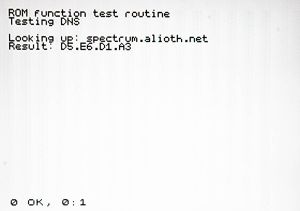
Today, my 128K toastrack made its first ever DNS lookup.
The DNS function call opens a UDP socket from the library I've been writing, assembles a DNS message, sends it, and interprets the response. It's not finished: the timeout mechanism must be added, as well as the ability to query another nameserver if the first one doesn't give any joy (has failed, or perhaps doesn't know the answer to the query).
The DNS routine is basically to do lookups for the eventual 'gethostbyname' call. As such, it'll only retrieve "A" resource records (i.e. map hostnames to IP addresses); it ignores all other parts of a DNS answer. It's quite unlikely anyone's going to want to do any other kind of DNS lookup on a Sinclair Spectrum, and anyway, it'll always be possible to write a little application to do deeper queries if someone really wants to do it on a Spectrum.
The other milestone this brings is that it's the first time the Spectranet has gone out onto the Internet, and poked a host that's not on my LAN. Specifically, my ISP's recursive DNS server. It also means that once gethostbyname() is written, the socket library supports what's needed for about 98% of socket-using programs - and I can do the Z88dk 'C' wrapper, so that programs written in C can use it, too.
I've also just got hold of a Spectrum +3. This will be used next week for basic hardware compatibility tests (such as the paging mechanism), and allow me to finish off the hardware schematic. Once I've done that I'm going to take a break from the software, since I now have enough to run tests that covers all aspects of the hardware. I will be looking at verifying the schematic makes sense, then allocating the CPLD pins, then laying out the first version of the PCB. Hopefully it'll be the only version of the PCB required, but I'm always mindful that the design might get improved as time goes on. Once the PCB is laid out, I'll probably get a batch of five or so made up.
Winston 19:51, 9 March 2008 (UTC)
UDP
As a relief from working on the interpreter, I decided to finish off the basic socket library, and test UDP. It went relatively painlessly - I just had to correct some false assumptions I had made about the hardware. So now I've successfully opened a UDP socket, and test the sendto/recvfrom functions.
This paves the way for writing the DNS routines such as gethosbyname to turn a hostname into an IP address. So I'll have to read and inwardly digest the gory details of the DNS protocol by reading the RFC.
Next week I'm going to take a break from the software, and start working on the PCB layout for the prototypes. The first step will be to decide the final pinout for the CPLD, which will largely be determined by trying to make the PCB layout as easy to route as possible (so the address and data bus pins are likely to be laid out in a way such that it's a straight shot to the edge connector). I also bought a ZXCF interface to test with the Spectranet prototype. I already need to change my port addresses (I knew this anyway) to avoid any conflicts. To recap, I'm going to have to take the slightly unconventional method of using the upper half of the address bus as the variable part of my port address to be compatible with all the mass storage devices I want to be compatible with.
Some basic frustration
I thought I'd take a look at ZX BASIC extensions. It's been a very frustrating experience. While I have the simple commands for loading new stuff into memory/flash over ethernet, they don't actually work correctly within the context of the interpreter.
Using the Complete Spectrum ROM disassembly and the IF1 disassembly, I set out to find out how it's done properly, but I've just not seen the wood for the trees. It feels like I've made zero progress. It doesn't really help that I've not had much time this week to work on it, either. I want to use these disassemblies to understand HOW the interpreter works, and how the IF1 extends it - not copy code as firstly this would infringe copyright, and secondly, just copying code doesn't make me understand it.
I'd really like a high level view of how the interpreter works, and what system variables to prod to make it do the right thing after the successful handling of a command, and do the right thing so that I can call functions in the ZX ROM to do things like parse arguments. (Unrecognised commands work just fine). I did make a test framework which allows me to load a program over ethernet as an interpreter extension to try stuff out - but that's the only positive progress I actually made. The trouble I'm having is the parser gets called twice after I've supposedly told the ZX ROM that all is done, and also that getting parameters using the ZX ROM doesn't work at all.
The interpreter extensions themselves are to be implemented in the standard way (trap RST 8 when the main ROM fails the command, then see if it's one for us).
To make myself feel better by making actual progress, I might look at the W5100's UDP capabilities next week and do some more final tweaks to the CPLD.
Mulling over the PCB layout
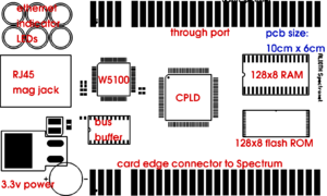
This evening, I decided to have a look at component placement, and see if I want to do is actually possible. My target is for a PCB no larger than 100mm by 60mm. For a board that sticks out of the back of the Spectrum (rather than going underneath, a la Interface 1), there are size constraints. The right hand side of the PCB can't overhang the edge connector by much or you'll never get the 9v power plug in. On the left, you can't go too far or you get in the way of the MIC/EAR plugs on the 48k, or in the way of the RGB cable on the 128k toast rack. I don't own an Amstrad Spectrum so I don't yet know of any additional size constraints it'll bring. As for the depth of the board, 6cm is about the most without causing mechanical problems if stuff is connected to the edge connector.
This means the board will be extremely dense. To get an idea, look at the mock up on the right. It doesn't look too bad till you view it actual size.
This is going to be a challenging PCB to lay out, it'll probably be several days work to do it. It must be at least 4 layer; the board would be twice the size to do it with two, and the through port would have to be much more complex (that makes it expensive). Around the W5100 things get hairy: traces for the through port must avoid the 25MHz crystal (not shown, but it'll be above the W5100), and also the analogue supply for the W5100...which sits right between the 4 left most edge connector pads. On the flip side, 4 layers is a huge luxury (I'm used to doing everything with two) as well as targeting a manufactured board rather than a home made board. A manufactured board means I can use far smaller vias, and I can put them underneath surface mount chips. Having a 4 layer board also means that I will have a proper ground plane for a change, which will make the W5100 perform much better (it's sort of marginal on my 2 layer home made breakout board). Even with the proper ground plane and better decoupling that I can do with a factory made PCB, I'm still going to keep the 74HCT245 buffer on the W5100's data bus - it would be a false economy to delete it. Horowitz and Hill in their book, The Art of Electronics always admonish their students to design for the worst case.
Hardware finalization and core library testing
Hardware
The last few days have been adding the bits to the CPLD that are shown in the schematic, but not actually added to the hardware I have on my work table. In particular, I've added the global execution trap enable input. The point of this is to allow for the assembly of new boards using a Spectrum as the flash programmer. When building a board, the first thing that has to be done is to configure the blank CPLD. The flash, being surface mount, can't be programmed until it's soldered onto the board, so immediately after the CPLD is configured, you've got no ROM. What would happen on power up is that the Spectrum would immediately crash - the RESET condition would be trapped, but the entirety of the flash ROM would be nothing but RST 0x38 instructions. So there needs to be some way of disabling the execution trap - the simple way is to have a jumper that allows you to disable the trapper (but leave all other functions enabled). Then the ROM image can be flashed, perhaps loaded from tape, but in my case, I'll put it on an IDE device connected to a DivIDE on the through port.
I've made some other changes, such as changing the HOLD ROMCS pin to an open drain output. This means only one P-channel MOSFET is required to do the 3.3v to 5v level shift to hold ROMCS high when the ROM is paged in (rather than the previous scheme that used two transistors). As well as slightly reducing the component cost, it opens up more space for trace routing on the board.
Partial port decoding is teh suck. Unfortunately, Sinclair did it a lot, and it got me in trouble when I connected the 128k toast rack Spectrum to the prototype. The ports I'm using, if the upper half of the address bus wasn't set just right conflicted with the 128k memory paging, causing an instant crash. This could be fixed in software (by using OUT (c), r, and setting B to 0x80). But the trouble is, it's very very hard not to conflict with some piece of hardware due to the number of devices that only check one or two bits out of the 16 available.
I also found out that the Plus D was using a lot of ports, some directly conflicting with mine, too. I would like this board to work with the Plus D (I'd really like to have it work with the DivIDE, DivIDE+, Plus D, ZX Interface 1, and the 128k +3's disc drive). To do this it's looking increasingly like I won't be able to have my I/O ports in the lower 8 bits; I'll probably have to use ports 0xF0FF, 0xF1FF, 0xF2FF and 0xF3FF for the 4 I/O ports I need. Since I'm already going to have to do LD BC, port/OUT (c), r anyway, even if using the lower address bus, the slightly unconventional port usage won't really hurt.
I've also been pricing up PCBs. In quantities of 50, the price for a 4 layer board vs. a 2 layer board is really not much more (once you add the through port - a 4 layer board with a simple edge connector on the back, vs a much larger 2 layer board with a riser for the through port like the DivIDE+ - a 4 layer PCB is less expensive), so I'm pretty convinced a 4 layer PCB is the way to go. It'll allow for a decent ground plane even ignoring the extra routing options the extra two layers will allow. I need to mock up some designs in PCB to see how it will all fit together, probably some time next month. If Rich Mellor can sell 100 DivIDE+ systems, I don't think I'm taking a huge financial risk if I order up boards 50 at a time from PCB Train.
Software
I've been debugging the code I wrote on the plane to Houston. What I did is made a simple test program, that assembles all the W5100 routines into RAM, and tests them in RAM. Then I just load this program into RAM using the *F command I added to the experiment ROM (which I currently have loaded). It's very handy - I can just sit at my Linux workstation, add some test code, assemble, type *F on the Spectrum and use the 'ethup' utility to send the program over the ethernet cable to the Spectrum. Run the tests, then reset the Spectrum for the next test. It makes it very fast to try out the code on the real hardware, since the test program loads instantly over ethernet.
The code mostly worked, but there were a few bugs that needed to be fixed, most of them pretty simple and caused by omissions, rather than discovering something really broken about the design.
The library test routines so far can be viewed in WebSVN here [1]. So far, this tests some of the core routines - opening and closing sockets, receiving and sending data over a TCP socket.
I want to get the basic TCP and UDP code tested before I get the prototype PCBs made, to ensure there are no bad showstoppers with the current breadboard prototype, so that's why I've got some focus on the software before the first PCBs have been made.
Winston 21:33, 24 February 2008 (UTC)
A solidification of the plans
While I've been away, I've not quite completely left things alone.
For example, I had quite a bit of time in planes and stuck in airport terminals. My 12in. Apple PowerBook is not only small - fitting neatly into a pocket of my backpack (I've never seen the need for a laptop bag, they scream 'Steal Me!') - but also runs gschem just fine.
So I passed the time on the plane from Houston to Salt Lake City and back making symbols for the memory and the W5100, and also experimenting with transforming a schematic into a netlist and PCB layout with my own symbols. Then, I made the CPLD symbol, and on the plane from Houston to Gatwick, started on the schematic proper. I nearly missed the plane from Gatwick back to the Isle of Man, I got so engrossed.
If you go to the image on the right, make sure you download it and zoom in fully, it's about 3000x2000 pixels or so - with so many pins on the chips the schematic gets a bit large. On this schematic, I'm explicitly showing power pins (often, people omit them from schematics). There are no less than 3 voltages used - 5v, 3.3v and 1.8v, as well as analogue 3.3v and analogue 1.8v - no less than 5 power nets. Also, there's a bit more than the usual decoupling used, so I want to show this explicitly. (I'll modify gschem's 74245 symbol to include power). It's a work in progress and not yet complete; in particular, I've not yet decided the pin assignments for the CPLD, nor the precise details of the reset circuit, and I need to finalise the ROMCS circuit (and have it compatible with the Spectrum +3). The through port is not shown on the schematic (and I don't intend to show it, except for indicating where A15OUT should connect).
Once the final prototyping is complete, and I've tested the basic socket library (to shake out any hardware problems I've not yet discovered), the next step will be the PCB. I intend to make 10 prototypes, using PCB Train as a board maker (the same board maker used for Papaya Labs DivIDE). My plan for the PCB is to make it pretty small - around 10cm by 5cm - if I can keep it short, then the through port can be just on the back of the PCB. This may require a 4 layer board.
While in Houston, I visited EPO - it's a handy component shop with all sorts of interesting stuff. I picked up a few 74HCT245 ICs while I was there - if you read down to some older entries here, you'll see the problems encountered with when 0xFF is read from the W5100 - which doesn't have the oompf to drive the Spectrum's long bus (with all the parasitic capacitance that implies). The '245 allows me to separate the Spectrum's bus from the W5100's data I/O pins, so the W5100 is only driving the lines to that one chip, with nice high impedance FET inputs. Putting the '245 on the breadboard completely solved the problem, even after removing all the 4.7k pull up resistors. I've decided I'll use the '245 rather than putting a bidirectional buffer into the CPLD, since the bidirectional buffer uses a heap of macrocells (about 25!) I could use for something that would take several chips to implement.
Winston 21:55, 19 February 2008 (UTC)
