Difference between revisions of "Memory"
(New page: == Overview == thumb|right|300px|Spectranet hardware memory map into the lower 16K The Sinclair Spectrum unfortunately doesn't have a formal sideways memory scheme. ...) |
|||
| (6 intermediate revisions by the same user not shown) | |||
| Line 5: | Line 5: | ||
The Sinclair Spectrum unfortunately doesn't have a formal sideways memory scheme. Instead, we just have the ability to page in external memory into the lower 16K of the Z80's address space, then manage this ourselves. Memory management is carried out by the [[Spectranet CPLD|CPLD]], which looks after which pages are mapped where, and when to page in our memory map into the lower 16K address space. | The Sinclair Spectrum unfortunately doesn't have a formal sideways memory scheme. Instead, we just have the ability to page in external memory into the lower 16K of the Z80's address space, then manage this ourselves. Memory management is carried out by the [[Spectranet CPLD|CPLD]], which looks after which pages are mapped where, and when to page in our memory map into the lower 16K address space. | ||
The Spectranet memory is arranged in 4K pages, with up to 4 chips | The Spectranet memory is arranged in 4K pages, with up to 4 chips, each chip a maximum of 256K in size (the actual hardware uses a 128K flash ROM, a 128K static RAM and the W5100's 32K buffer). The flash ROM is chip 0, the W5100 is chip 1, chip 2 is unused at present and chip 3 is the static RAM. Two pages are permanently mapped into the lowest 4K (flash ROM) and highest 4K (static RAM). This is to guarantee to software that certain memory will always be in the same place; page 0 of flash is used to contain initialization routines, the socket library and interrupt handlers. Page 0 of the static RAM is to hold general purpose workspace, system variables, and the jump table. | ||
The middle 8K of this area is the paged area. Any page of any chip can be paged into page area A (0x1000 to 0x1FFF) or page area B (0x2000 to 0x2FFF). | The middle 8K of this area is the paged area. Any page of any chip can be paged into page area A (0x1000 to 0x1FFF) or page area B (0x2000 to 0x2FFF). | ||
This arrangement allows for 1MB of addressable memory (page 00:000-FF:FFF). In this scheme, the lower permanently mapped page is 00:000 - 00:FFF, and the upper permanently mapped page is C0:000 - C0:FFF. The following diagram shows how the address space is laid out in detail: | |||
[[Image:Address-space.png|thumb|center|800px|Key: Red = flash ROM. Yellow = W5100. Blue = static RAM. Grey = no connected hardware]] | |||
== Selecting pages for the paged area == | == Selecting pages for the paged area == | ||
Two registers are provided for selecting pages - page register A, which contains the page for 0x1000 to 0x1FFF, and page register B for 0x2000 to 0x2FFF. These are 8 bit registers, and allow access to 256 4K pages (a total of 1MB of address space). The two most significant bits are demultiplexed by the CPLD to provide four chip select signals (thus dividing the 1MB of address space amongst up to 4 chips). This means that to select flash ROM, set the page register to a value between 0x00 and 0x1F. To select the W5100's buffers, the page register should be a value from 0x40-0x48. The RAM is selected with a page register value of 0xC0-0xDF. | |||
The following I/O ports are used ('''important''' - these may change during prototyping): | |||
* Port 0x003B - Memory page for area A (8 bits) | |||
* Port 0x013B - Memory page for area B (8 bits) | |||
The complete 16 bits of the port address is decoded, so only OUT instructions to these specific ports will work (unlike older peripherals, which tend to only decode at most 3 bits of a port address). The paging registers are write-only; the currently selected page should be stored in the system variables area. | |||
Functions are provided in ROM to perform paging; it should not be necessary to use OUT instructions directly to select the pages. Two types of paging routine are provided: a simple routine that performs paging and keeps the system variables updated with the currently selected page, and routines that in addition to that, push the last page onto the stack. A matching routine pops the page off the stack and restores it. | |||
TODO: A routine will be provided to allow for "longcalls" (page in a specific page, and call it, and restore on return). | |||
== ROM Memory Map == | |||
Most of the flash ROM is available for developers to use for their own purposes (see [[Writing Spectranet ROMs]] for more information). There are 32 4k pages (pages 0x00 to 0x1F) available. The following pages are reserved for the Spectranet itself: | |||
* Page 0x00 - Permanently mapped to 0x0000-0x0FFF. This contains the socket library and utility function calls. | |||
* Page 0x01 - Spectranet data. | |||
* Page 0x02 - Spectranet utility programs - configuration utility and DHCP client. | |||
* Page 0x03 - Reserved for future use. | |||
* Last 256 bytes of page 0x1F - Storage for Spectranet configuration. | |||
== RAM memory map == | |||
Most of the static RAM is also available for developers, however, some is reserved: | |||
* Page 0x00 - Permanently mapped to 0x3000-0x3FFF. Contains temporary workspace, buffers, and system variables. Some of this is available to developers; see below. | |||
Pages 0x01 and 0x02 are used to store a copy of the Spectrum's frame buffer when an NMI or similar event is triggered. Pages 0x1C-0x1F are used by the configuration utility when rewriting the last erase sector of the flash rom, while updating the configuration. | |||
[[Category:Spectranet]] | [[Category:Spectranet]] | ||
Latest revision as of 22:08, 28 June 2010
Overview
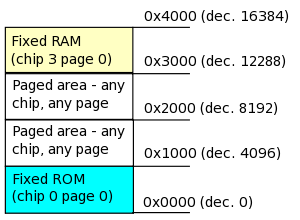
The Sinclair Spectrum unfortunately doesn't have a formal sideways memory scheme. Instead, we just have the ability to page in external memory into the lower 16K of the Z80's address space, then manage this ourselves. Memory management is carried out by the CPLD, which looks after which pages are mapped where, and when to page in our memory map into the lower 16K address space.
The Spectranet memory is arranged in 4K pages, with up to 4 chips, each chip a maximum of 256K in size (the actual hardware uses a 128K flash ROM, a 128K static RAM and the W5100's 32K buffer). The flash ROM is chip 0, the W5100 is chip 1, chip 2 is unused at present and chip 3 is the static RAM. Two pages are permanently mapped into the lowest 4K (flash ROM) and highest 4K (static RAM). This is to guarantee to software that certain memory will always be in the same place; page 0 of flash is used to contain initialization routines, the socket library and interrupt handlers. Page 0 of the static RAM is to hold general purpose workspace, system variables, and the jump table.
The middle 8K of this area is the paged area. Any page of any chip can be paged into page area A (0x1000 to 0x1FFF) or page area B (0x2000 to 0x2FFF).
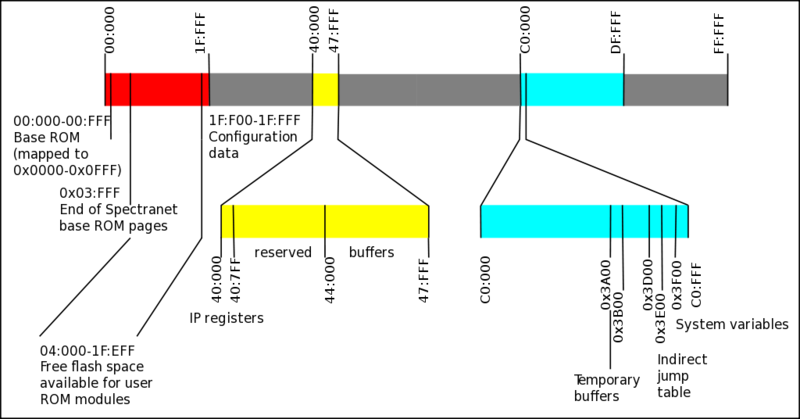
This arrangement allows for 1MB of addressable memory (page 00:000-FF:FFF). In this scheme, the lower permanently mapped page is 00:000 - 00:FFF, and the upper permanently mapped page is C0:000 - C0:FFF. The following diagram shows how the address space is laid out in detail:
Selecting pages for the paged area
Two registers are provided for selecting pages - page register A, which contains the page for 0x1000 to 0x1FFF, and page register B for 0x2000 to 0x2FFF. These are 8 bit registers, and allow access to 256 4K pages (a total of 1MB of address space). The two most significant bits are demultiplexed by the CPLD to provide four chip select signals (thus dividing the 1MB of address space amongst up to 4 chips). This means that to select flash ROM, set the page register to a value between 0x00 and 0x1F. To select the W5100's buffers, the page register should be a value from 0x40-0x48. The RAM is selected with a page register value of 0xC0-0xDF.
The following I/O ports are used (important - these may change during prototyping):
- Port 0x003B - Memory page for area A (8 bits)
- Port 0x013B - Memory page for area B (8 bits)
The complete 16 bits of the port address is decoded, so only OUT instructions to these specific ports will work (unlike older peripherals, which tend to only decode at most 3 bits of a port address). The paging registers are write-only; the currently selected page should be stored in the system variables area.
Functions are provided in ROM to perform paging; it should not be necessary to use OUT instructions directly to select the pages. Two types of paging routine are provided: a simple routine that performs paging and keeps the system variables updated with the currently selected page, and routines that in addition to that, push the last page onto the stack. A matching routine pops the page off the stack and restores it.
TODO: A routine will be provided to allow for "longcalls" (page in a specific page, and call it, and restore on return).
ROM Memory Map
Most of the flash ROM is available for developers to use for their own purposes (see Writing Spectranet ROMs for more information). There are 32 4k pages (pages 0x00 to 0x1F) available. The following pages are reserved for the Spectranet itself:
- Page 0x00 - Permanently mapped to 0x0000-0x0FFF. This contains the socket library and utility function calls.
- Page 0x01 - Spectranet data.
- Page 0x02 - Spectranet utility programs - configuration utility and DHCP client.
- Page 0x03 - Reserved for future use.
- Last 256 bytes of page 0x1F - Storage for Spectranet configuration.
RAM memory map
Most of the static RAM is also available for developers, however, some is reserved:
- Page 0x00 - Permanently mapped to 0x3000-0x3FFF. Contains temporary workspace, buffers, and system variables. Some of this is available to developers; see below.
Pages 0x01 and 0x02 are used to store a copy of the Spectrum's frame buffer when an NMI or similar event is triggered. Pages 0x1C-0x1F are used by the configuration utility when rewriting the last erase sector of the flash rom, while updating the configuration.

